
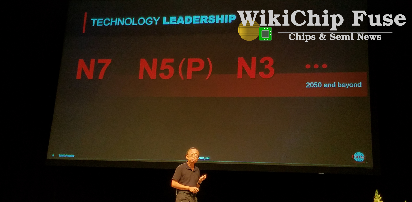
TSMC Details 5 nm
For the past decade, TSMC has been operating at a fairly consistent cadence. The company started risk production of its latest node, 5-nanometer, in March 2019. 5-nanometer is expected to ramp around the second quarter of this – likely April or May timeframe as long as COVID-19 does not disrupt operations. This article sources its information from a number of places including Arm Techcon 2019, 65th IEEE IEDM conference, and ISSCC 2020. We are also a little disappointed that, despite the significance of the paper, TSMC’s IEDM paper lacked real substance and was accepted without meeting the conference high quality standard we have come to expect from IEDM.
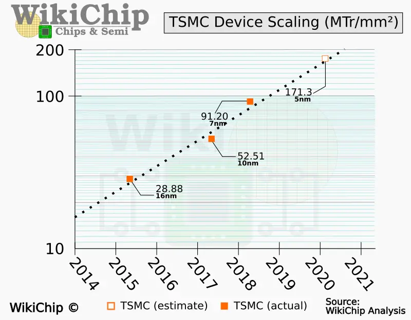
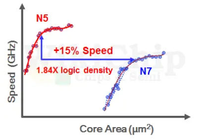
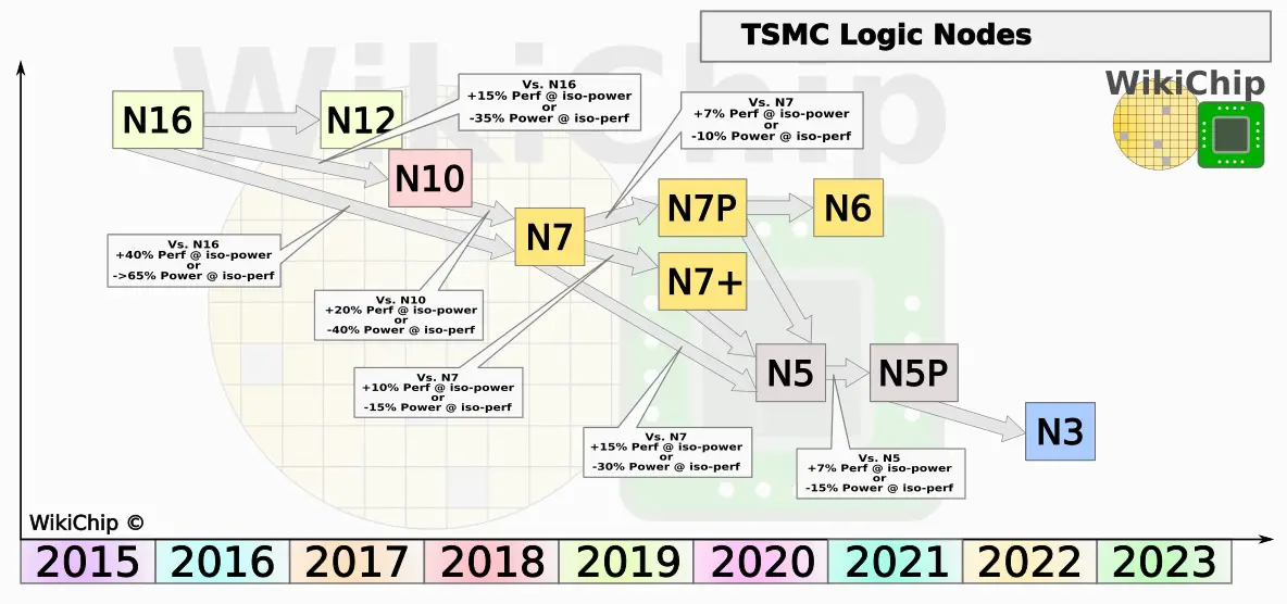
TSMC has yet to disclose the exact device sizes for the N5 node, therefore we will stick to our own estimates. Our current estimates remain at 48 nm poly pitch and 30 nm metal pitch. Those dimensions yield an estimated device density of 171.3 MTr/mm². At IEDM, TSMC reported 1.84x density improvement over the company’s own N7 node. Our estimates land at 1.87x which is reasonably close. The comparison isn’t perfect as they are comparing the density of a whole CPU block and we are not, but the numbers are reasonably close based on the available information. A ramp in April will mark exactly two years since TSMC ramped its 7-nanometer node. Impressively, it’s also just under 5 years since the company ramped its 16-nanometer node, their first FinFET device. From N16 to N5, TSMC is currently pushing out production nodes at Moore’s Law pace of 2x/2 years which is actually faster than the historical trend line.
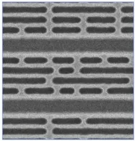
In one of the figures in the IEDM paper, TSMC had an illustration of patterning fidelity of EUV. It’s hard to tell how much we can rely on the visuals that were attached to the IEDM paper but if we were to assume that the minimal metal pitch here is roughly 30 nm, the cell height is roughly ~6T (identical to N7) which works out to around a 180 nm cell height. The high-density cells are likely 2+2 yielding 8-fin high cells, but if the COAG meant a single-fin isolation, N5 might be 7-fin high. In other words, the fin pitch is likely 25-26 nm. TSMC did mention that there is an HPC cell variant which uses 3 fins. If we assume a 25 nm FP, the HPC cells are 225 nm tall or 7.5T (also identical to N7).
Below are our current assumptions based on the available data.
| Estimates for N5 | ||
|---|---|---|
| Cell | HD | HP |
| FP | 25 nm | |
| MxP | 30 nm | |
| Device | 2+2 | 3+3 |
| Height | 175/180 nm 6T |
225 nm 7.5T |
PPA
At a high level, TSMC N5 is a high-density high-performance FinFET process designed for mobile SoCs and HPC applications. Fabrication makes extensive use of EUV at Fab 18, the company’s new 12-inch GigaFab located at the Southern Taiwan Science Park. TSMC says that its 5-nanometer process is 1.84x denser than its 7-nanometer node. TSMC also optimized analog devices where roughly 1.2x scaling has been achieved. At IEDM, Geoffrey Yeap gave a little more color to that density by reporting that for a typical mobile SoC which consists of 60% logic, 30% SRAM, and 10% analog/IO, their 5 nm technology scaling was projected to reduce chip size by 35%-40%.
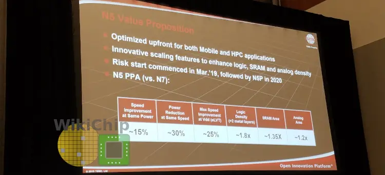
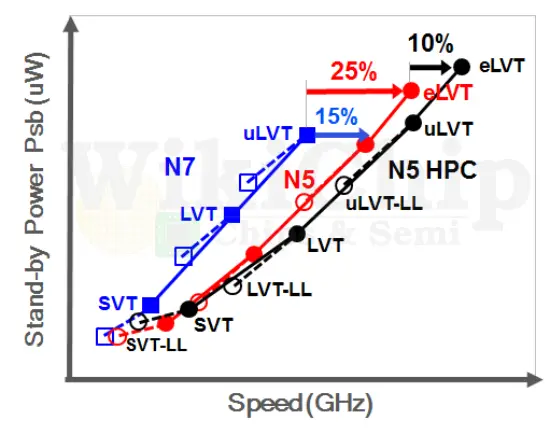
From a device power and performance perspective, TSMC says devices offer 15% higher speed at iso-power or, alternatively, 30% lower power at the same speed. These numbers are consistent with what was reported previously.
In addition to the ultra-LVT (uLVT) that was offered with N7, there is a new extreme-LVT (eLVT) which can push that 15% up to 25% higher speed. Additionally, compared to the standard N5 cells, the HP cell variants which we mentioned above can push that performance by another 10% at the cost of density.
EUV
TSMC emphasized the extensive use of EUV with this process. It’s worth pointing out that this is really TSMC’s first ‘main’ EUV-based process. TSMC N7 and N7P nodes are DUV-based. TSMC first production EUV process is the N7+ but that node is really an orphan – not compatible with the prior nodes and no clear migration path forward other than going back to this node. On the other hand, N5 is designed as the main migration path from N7 for most customers. TSMC says that more than 10 EUV layers are used to replace at least 4 times more immersion layers at cut, contact, via and metal line steps. This is comparing their EUV-based N5 node to a hypothetical N5 node that utilizes multi-patterning.
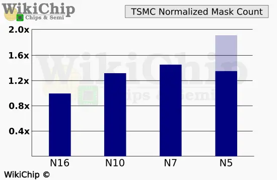
At IEDM, TSMC showed a graph reporting that, for the first time, N5 will result in fewer masks than the prior process. Measuring out the height of the bars in the graph, compared to the baseline 1x N16, N10 uses 1.31x more masks, N7 uses 1.45x more masks, and N5 uses 1.35x more masks. If N5 was a multi-patterning DUV-based process, the mask count would have ballooned up to 1.91x. In other words, with 14/16nm using around 60 masks, 10 nm is roughly 78 masks, 7 nm is roughly 87 masks, and 5 nm is back down to 81 masks. Without EUV, 5 nm would have been at 115 masks. No comparison to N7+ was given but we estimate it to be comparable to the 10 nm mask count.
HMC
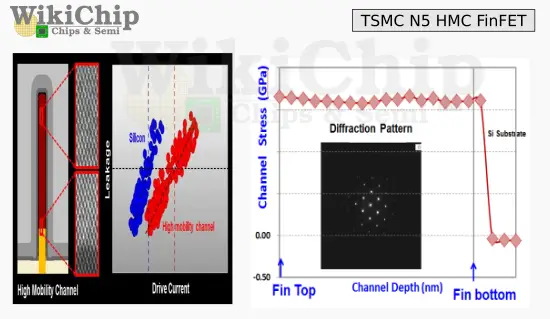
In order to improve the drive current, TSMC introduced a high-mobility channel (HMC) for its 5-nanometer FinFET devices. TSMC made every effort to avoid detailing the actual properties of that channel (every related question was met with the tautology: “those who know, know”). It’s a fruitless endeavor to try to hide such generic information. We expect TechInsights to publish that info within a few months after products start shipping. We believe TSMC is employing a SiGe channel for the pMOS devices. The number we heard being thrown around is around a 37% Ge composition. TSMC says that the HMC delivers 18% performance gain versus equivalent Si finFETs. A TEM of the full-strained HMC lattice is shown below.
Scaling Boosters
TSMC says it has incorporated a number of scaling boosters in its N5 process. Interestingly, TSMC is calling them “smart hyper scaling features”, a marketing term previously used by Intel. The first booster is what TSMC is calling “unique diffusion termination”. We believe this is referring to some form of a single diffusion break at cell boundaries. Additionally, TSMC added the ability to drop the gate contact over the active region (COAG). Both features were previously introduced by Intel on their 10-nanometer node as part of their ‘hyper-scaling features’.
Interconnect
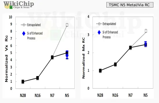
Despite aggressively tighter pitches, TSMC says metal lines RC and via resistance have been kept relatively similar to N7. TSMC says this was achieved by “using EUV patterning, innovative scaled barrier/liner, ESL/ELK dielectrics, and Cu reflow.” The improvements meant the interconnect RC did not worsen relative to N7 as N7 did relative to N16.
SRAM
TSMC disclosed two 6T SRAM variations: a high-performance cell and a high-density cell. The high-performance cell is 0.025 µm² while the high-density cell is 0.021 µm². Both cells are the densest SRAM cells reported to date in both absolute footprint and in their respective categories. In other words, even the high-performance SRAM cell is denser than all other SRAM cells reported to date that are in production.
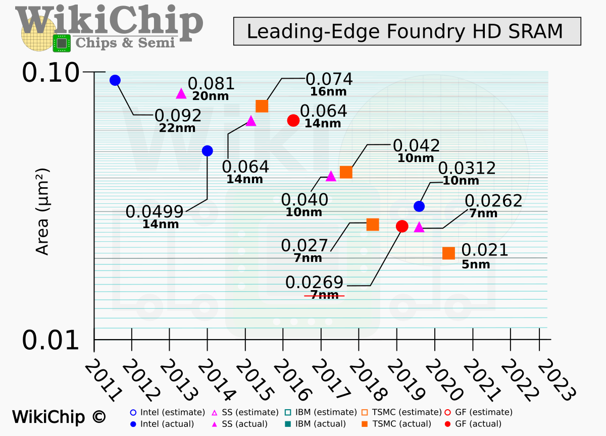
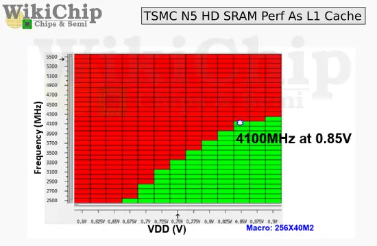
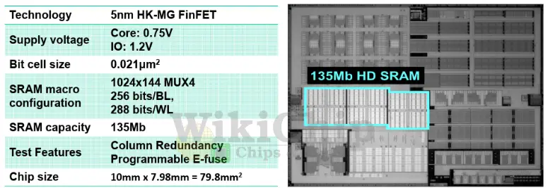
Previously we assumed a ballpark assist circuit overhead of around 30% which yielded an estimate of ~32 Mib/mm² of cache. This an increase of 30% from N7 which is around 24.7 Mib/mm². At ISSCC 2020, TSMC presented a test shuttle with 135 Mib of HD SRAM and additional IPs. Their reported density for the HD cells did in fact match our estimates. A Shmoo plot of the HD SRAM array was shown where it was used as high-performance L1 caches. They were able to achieve 4.1 GHz at 0.85 V. A closer look at the graph reveals that if they were to push the voltage higher to 0.9 V they can get past 4.2 GHz.
Final Thought
TSMC execution has been remarkable the last couple of nodes. Since their 16 nm node, each process node has been ramping quicker than its predecessor. N7 was the company’s quickest-ramping node with fastest defect density reduction ever. TSMC says it expects its N5 node to ramp even quicker. 5-nanometer entered risk production in March 2019. The process is expected to ramp in Q2 this year – likely in April or May. When ramped, this will be the densest process in terms of both transistor density and SRAM density – leapfrogging both Samsung and Intel. Samsung 5-nanometer is only slightly denser than their 7-nanometer and is not competitive with TSMC 5 nm. Samsung’s next big jump is their 3-nanometer node. Intel will likely capture the density lead with their 7-nanometer node, however, that node isn’t coming until late next year – a solid 1.5 years behind.
TSMC 5-nanometer node will be ramping at Fab 18, a new 12-inch EUV GigaFab being constructed in three phases. Phase one finished in early 2018 which is where 5-nanometer is ramping. Phase 2 started a little later and is expected to enter volume production in 2020 as well. The final phase, Phase 3, started in 2019 and is planned for volume production in 2021. Fab 18 will also be the future home of their 3-nanometer process which is planned for 2022.
Beyond the process technology itself, TSMC is also working on the packaging side. CoWoS is currently the company’s main 2.5D technology. Recently TSMC announced 2x reticle CoWoS with up to 2.7 TB/s of HBM bandwidth particularly optimized for the 5-nanometer node. In the future this will be extended to 3x reticle and up to eight HBM stacks. TSMC also announced the SoIC packaging which is the company’s 3D stacked packaging technology.
–
Spotted an error? Help us fix it! Simply select the problematic text and press Ctrl+Enter to notify us.
–